PCO
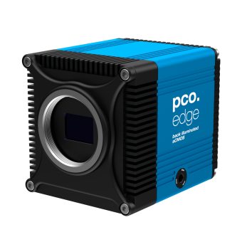
Pioneering in Cameras and Optoelectronics (PCO) has been our shared philosophy since our establishment in 1987. Starting with image-intensified cameras, followed by the co-invention of the groundbreaking sCMOS sensor technology, PCO greatly surpassed the imaging performance standards of the day. Acquired by Excelitas in 2021, our PCO camera portfolio continues to forge ahead as leaders in digital imaging innovation across diverse applications such as scientific and industrial research, automotive testing, quality control, and metrology.
With sophisticated mechanical design, extensive software support, and a broad range of accessories, we deliver adaptable solutions for all demands. This adaptability extends to tailor-made firmware and custom image sensors, which allow us to develop highly specialized solutions for all our customers. PCO represents a world-renowned brand of high-performance camera systems that complement Excelitas’ expansive range of illumination, optical, and sensor technologies and extend the bounds of our end-to-end photonic solutions capabilities.
Our comprehensive camera portfolio covers the entire spectrum - from deep ultra-violet (DUV) to shortwave infrared (SWIR), from long exposure to high-speed, from line scan to high-resolution area scan. Our camera systems are controlled and processed through an intuitive and powerful software suite addressing an extensive range of platforms and architectures.
The outstanding quality and high reliability make our products unique on the market. Please explore our selection guide on MachVis to find the perfect camera system for your application.
Need something better suited to your specific requirements?
Engage Excelitas to meet your most complex custom requirement.


